Our Solutions and Services.
SEMICONDUCTOR PRODUCT ENGINEERING.
Our Solutions and Services.
SEMICONDUCTOR PRODUCT ENGINEERING.
01 processing equipment
Wet Etch and Clean Equipment.
OUR EQUIPMENT PORTFOLIO COVERS SOLUTIONS FOR LOW, MEDIUM AND HIGH THROUGHPUT REQUIREMENTS TAILORED TO OUR CUSTOMER’S NEEDS.
All our wet chemical processors offer thin- and ultra-thin wafer processing capabilities and integrated metrology for substrate thickness and roughness measurements:

MG21 – Highly flexible single-wafer wet chemical processor for lower throughput requirements.
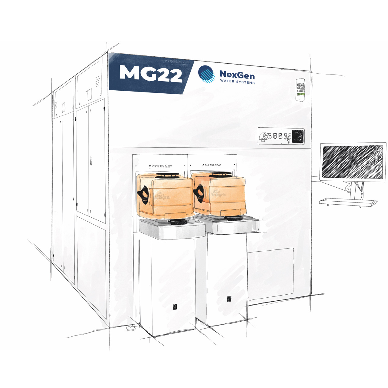
MG22 – Highly flexible single-wafer wet chemical processor for medium-throughput requirements.
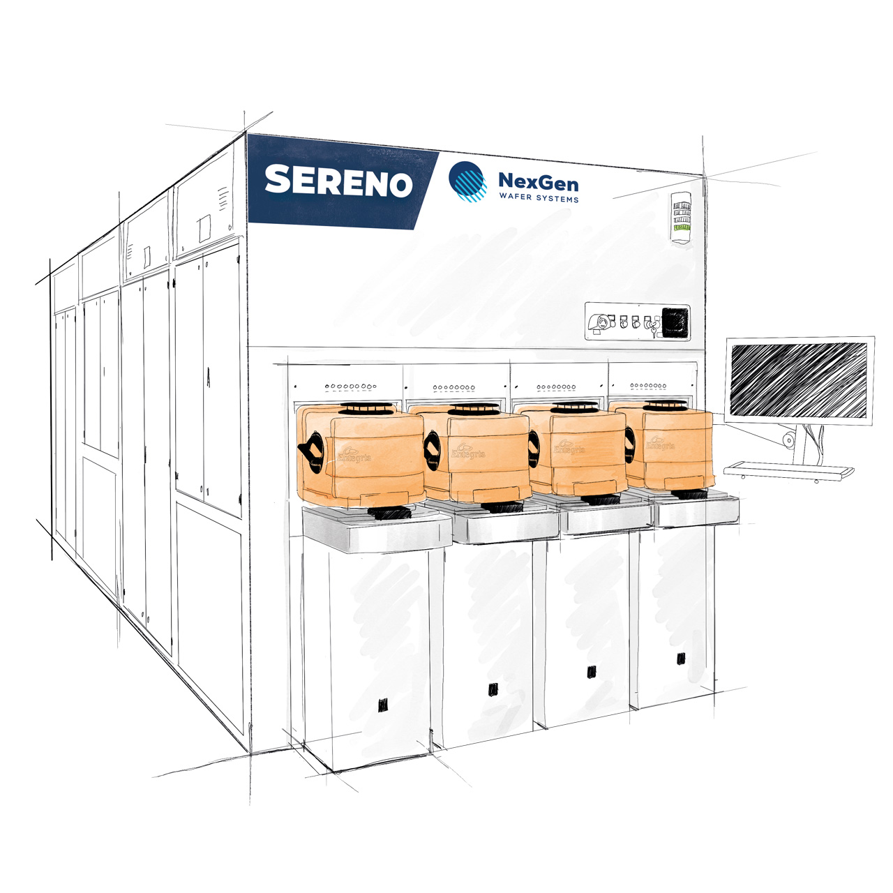
Sereno – Single wafer wet chemical processor for high throughput requirements.
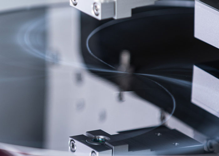
Thin wafer processing.
Our expertise in processing thin and ultra-thin substrates is our core competency and made us the market leader in this segment. Our versatile equipment platforms are capable of processing various substrate types and thicknesses. Silicon substrates, compound substrates (Sic, GaN, GaAs) and piezoelectric substrates with a thickness of less than 50µm and up to 2000µm and diameters from 3″ – 12″ can be processed on our equipment. Our ultra-thin wafer processing solutions allow carrier less processing of substrates with less than 50µm, also for 12″ substrates.
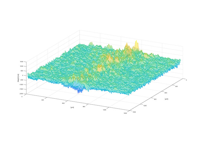
Integrated metrology.
Advanced process control incorporates real-time data acquisition and management of mission-critical process parameters that are vital to ensure maximum reliability and performance of semiconductors.
For manufacturing steps that require etch and clean processes, it is critical to monitor and control parameters that affect etch uniformity, repeatability, cleaning efficiency and total thickness variation in real-time. Our equipment offers these features to maximise process performance on a within-wafer and wafer-to-wafer basis. Our inline metrology solutions provide leading-edge process control for integrated surface roughness and substrate thickness in our process equipment.
02 Applications
Process Application Services.
ESTABLISHING AND QUALIFYING A NEW PROCESS IS A LONG AND CAPITAL-INTENSIVE PROCESS. WE HELP OUR CUSTOMERS TO OFFLOAD A PART OF THEIR DEVELOPMENT EFFORTS IN A COST-EFFICIENT WAY.
Our services include demo, pilot, and small-scale foundry services for process applications within our solution portfolio. Our highly flexible processing equipment provide a dedicated range of wet etch and clean applications for:

03 Bulk Chemical Supply & Blend Systems
Fluid Handling Systems.

OUR RANGE OF FLUID HANDLING SYSTEMS INCLUDES BULK CHEMICAL SUPPLY SYSTEMS AND BLEND SYSTEMS FOR WET CHEMICALS.
Bulk Chemical Supply Systems deliver chemistry to one or several wet process equipment. These flexible systems can be used for bulk chemistry supplies from as big as 1000 litres to smaller carboys with a volume of 5 litres.
Blend Systems blend and condition (heat and cool) wet process chemistries out of individual chemical components and supply them to process equipment. These systems blend multi-component chemistries with high accuracy in a cost-efficient way. Use cases are chemistries for silicon etch (substrate etch) and polymer removal (polymer clean) applications where highly accurate mixtures are required.
