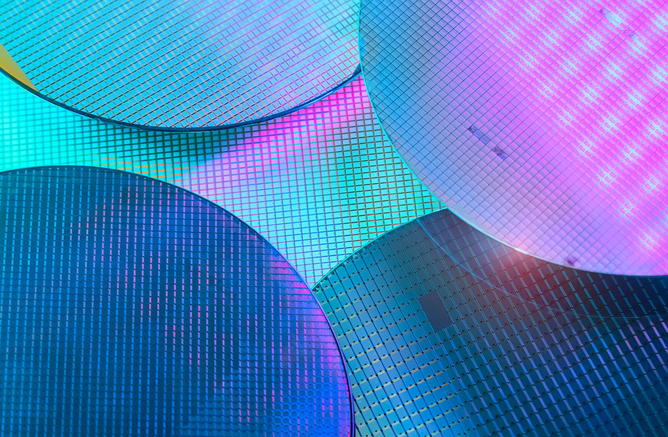
NexGen Wafer Systems Unveils Advancements in Ultra-Precise Wet Etching Powered by Integrated Metrology at SEMICON SEA 2025
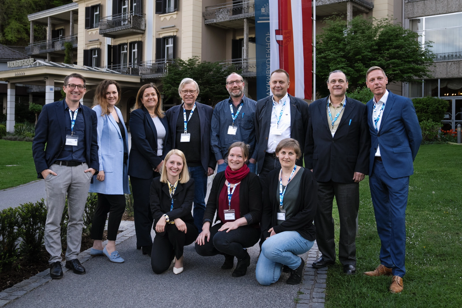
The event provided a platform for high-level discussions, insights into the latest developments, and intensive professional exchange. Representatives from various companies and research institutions shared their knowledge and experiences on the topics of Chemical and Mechanical Polishing (CMP) and wet chemical processing of semiconductor wafers (WET).