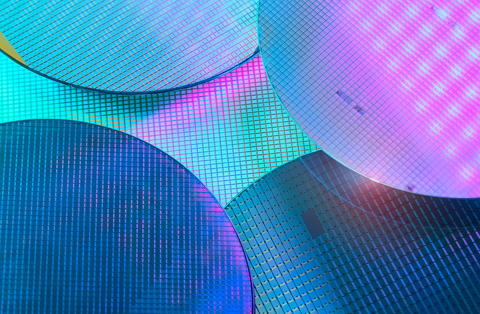
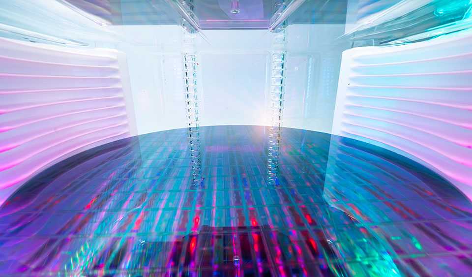
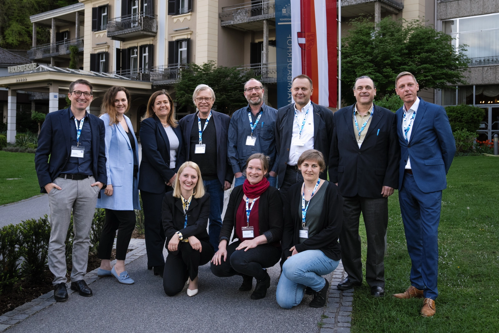
NexGen was Co-Organisator of the European CMP & WET Users Group Meeting

The event provided a platform for high-level discussions, insights into the latest developments, and intensive professional exchange. Representatives from various companies and research institutions shared their knowledge and experiences on the topics of Chemical and Mechanical Polishing (CMP) and wet chemical processing of semiconductor wafers (WET).

2024-06-27T16:04:12+02:00May 1, 2024|

Doping-selective etching of silicon for wafer thinning in the fabrication of backside-illuminated stacked CMOS image sensors

Backside thinning, using silicon doping-selective etching, for the preparation of backside illuminated (BSI) CMOS sensors. Tailored HNA chemistry (HF: HNO3: CH3COOH) is used to stop at a dedicated p+/p- silicon transition layer with high p+/p- selectivity, providing sub‑micron total thickness variation.

2024-06-17T10:50:02+02:00July 9, 2023|
Go to Top